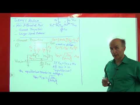
[1:27]Greetings. Welcome to Electronics 2. My name is Beza Razavi and this is lecture number 12. Today, we will extend our studies of the bipolar differential pair to the MOS differential pair. So we'll go over some general properties of this circuit, and then we will delve into its large signal behavior, meaning its input output characteristic, and see if we can derive an equation for it. Well, before we go there, let's just uh summarize what we did last time in the previous lecture. Okay, so and the previous lecture we uh tried to extend this notion of uh point of symmetry and AC ground in the small signal analysis of differential pairs. And we saw that, for example, even if you have degeneration resistors, this turns out to be a point of symmetry, so for small differential voltage changes here, this point is AC ground. So the circuit reduces to one half circuit like this, whose voltage gain can be readily written. And of course, we have seen this a number of times that the voltage gain of the half circuit, this, is the same as the differential voltage gain of the entire differential pair is the same expression. Okay. Uh then we looked at this example, where we have this just independent resistor connected between X and Y. And again, we tried to find the point of symmetry by breaking this into two halves and uh excuse me, providing an AC ground here. So, we saw that with this AC ground, I can readily write the voltage gain again for this half circuit here, right? Where these two are in parallel. But another important result was that, well, if this point is AC ground, and this point is AC ground, I can just connect them together. So now the circuit looks like this from a small signal point of view. Uh these terminals of these resistors are connected the same down here. Uh and these are called RL over 2, because we just got them from here. But then I thought, okay, I can change the name of the resistors. I change it to RO and that reflects the effect of early effect in these transistors. So, we saw that to find the voltage gain, again we just place RO in parallel with RC and multiplied by minus GM. Okay. Today, we will uh go to MOS differential pairs and see uh what we can do there. The MOS differential pair is very similar to the bipolar counterpart. Here's what we have. Two identical MOS transistors with a tail current source. And now we call this ISS, not IEE, SS means connected to source source, right? And then, these are called RD for the drain resistor on each side, and then we have two inputs and two outputs. So we would like to perform the same studies that we did for the bipolar pair here as well, but we don't really have to go through every detail because many of the concepts are similar. So we'll just proceed and explore. Okay. So, let's talk about the general properties. In the first case, like the bipolar differential pair, we just connect the inputs together and connect to a battery. Okay, so here's what we have. The differential pair. And I connect these two together and hold it at a battery voltage, some battery. And again, if you remember, we call this the input common mode level, VCM.
[5:49]Okay, we need some DC there, so they're just connected to some DC. For example, if the supply is uh let's say uh 1 volt, this could be maybe 0.8 or 0.7 volts, something like that. This battery. All right. Uh okay, so what's going on here in this case? Exactly. Well, if the circuit is symmetric and we see that M1 and M2 have the same gate voltages and the same source voltages, so this current has to split equally between M1 and M2. So again, like the bipolar differential pair, we have a current of ISS over 2 on this side and on this side, ISS over 2. All right, so that's pretty easy. Okay. Again, we are assuming that these transistors operate in saturation. Remember, for MOSFETs, we need to be in saturation, so that they have a high transconductance, they become good amplifying devices. So we're assuming that M1 and M2 are saturated. Okay. What else can we find here? Well, how much is VX and how much is VY? Well, the voltage drop from here to here is IS over 2 times RD. This is subtracted from VDD to give us the X, and same with VY. So VX is equal to VY, is equal to VDD minus RD ISS over 2. Okay, that's easy enough. All right. Now, here's the next question that we need to answer. How much is the VGS here? VGS1. Now we expect that, of course, these have the same VGS, because their gates are shorted and so are the sources. So VGS1 is the same as VGS2. How much is VGS1, if I know this current. All right. Well, let's look at M1. M1 is a MOS device. It is in saturation, and it has a drain current equal to ISS over 2. So I should be able to find the gate source voltage necessary for the transistor to carry that much current. And for that, I'm going to write my general equation. ID is equal to 1 half MU n c X W over L VGS minus VTH squared. Again, we are neglecting channel length modulation.
[8:38]Okay, so, uh for M1, which is in saturation, ID is equal to ISS over 2. So if I plug in ISS over 2, I can find VGS. So, I can say VGS1 is equal to, so this is ISS over 2. That factor of 1 half goes away with this. We divide by this, take the square root, and take VTH to the other side. So, that will give us ISS over mu n CX W over L plus VTH. Okay, so that's the gate source bias voltage of M1 and M2.
[9:27]We don't have any signals in differential signals coming in, so we have a some amount of current in the device, some amount of VGS. Those are the bias conditions. All right. Uh a few uh terms that we have used in the past, uh one is VGS minus VTH. So, I want to emphasize what this was called. So VGS minus VTH, this term itself is called the overdrive voltage.
[10:00]Okay, VGS minus VTH. That's the overdrive voltage. Uh one other term that we will use, uh actually I should have said it for the bipolar differential pair as well, but we'll say it here. So we say, if V in 1 is equal to V in 2, maybe approximately equal to V in 2. Well, okay, let me be precise, I'll just say they are equal for now. If they are equal, we say the differential pair is in equilibrium.
[10:52]Okay, this is true for the bipolar differential pair and for the MOS differential pair. It doesn't make any difference. But, uh, it's good to have a term for this because we repeatedly come back to this condition, where the gates are connected, so V in 1 minus V in 2 is 0, right? And we have some conditions that we have found for this case, for the equilibrium case.
[11:32]So it's good to remember that. Okay. But what's more curious is the term inside the square root. What's going on here? Uh this says that I have a positive number, minus a positive number. So if this positive number is large enough, it seems that these cancel each other, and ID1 minus ID2 goes to 0 again. Isn't that strange? We don't expect this circuit to do that, right? How could that be? As this voltage keeps increasing, uh this current monotonically wants to go to the left.
[12:44]Right? It's just uh the current prefers to go to the stronger MOSFET so to speak, so it keeps going to the left. And eventually all of the current should go flow flow from here. Why does that predict that something strange is going on? Okay. Well, the reason is that uh this equation is not valid for very large values of V in 1 minus V in 2.
[13:38]Okay, why? Well, because if V in 1 minus V in 2 exceeds a certain amount, then one transistor turns off. If one turns off, we can no longer write this equation for it. Remember, the quadratic equation that we had, 1 half mu n CX W over L VGS minus VTH squared is applicable only if the MOS device is on and in saturation. But when eventually one of these transistors turns off, we are no longer that equation is no longer valid. So this equation is valid up to some point, but beyond that point, we can't use this equation. And where is that point? How much V in 1 minus V in 2 can be tolerated before that equation breaks down? Well, we found the minimum V in 1 minus V in 2 that steered all this current to one side. On the previous slide, remember. So in that example, we spent some time and calculated the amount of current uh that the amount of voltage that was necessary. Remember the minimum voltage? And it looked like this.
[15:15]So, the minimum voltage necessary to steer all the current to one side is given by this value. If V in 1 minus V in 2 exceeds this value, M2 will be off. We can no longer write those equations for M2. So the big equation on next page is not valid anymore. So we're going to remember this. Okay, 2 ISS over something, right? So let's remember that and let's go back to the slide.


