[0:00]In this presentation, we are going to look at introduction to HDL.
[0:08]So the contents of this presentation are, what is HDL, Verilog HDL, and Verilog codes for a few circuits. So what is HDL? A hardware description language (HDL) is a language that describes any digital circuit in textual form. So usually we describe digital circuits using various logic gates and interconnections between them, right? So what HDL does is, it describes the same logic gates in a textual form using various notations. So the advantages of using HDL are, HDL can design describe a large complex design requiring hundreds of logic gates in a convenient manner, in a smaller space. So using hardware to implement some circuit, which you know consists of hundreds and hundreds of logic gates is very difficult to implement. And another advantage is, it uses software test-bench to detect functional error, if any, and correct it. This is known as simulation. So just imagine that you are implementing a circuit using a breadboard and a large number of ICs, which is very large. At the end of the implementation, if you find out that there's some error in your implementation, it becomes very difficult to pinpoint where the error is occurring, right? So in HDL, it uses software to detect where that error is occurring and if there is any error, it corrects it. And then, HDL gets hardware implementation details. This is also known as synthesis. So there are two widely used HDLs – Verilog and VHDL (Very high-speed integrated circuit Hardware Description Language). So Verilog is usually used and in this module, we are only going to discuss about Verilog codes. So what is Verilog HDL? So these this is some, you know, history about Verilog HDL. And Verilog HDL is kind of simple, you know. The reader with an exposure to any programming language like C will find it relatively easier to learn Verilog or any HDL.
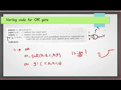
[2:34]Okay. So let's write our first Verilog test circuit, Verilog code for the test circuit. So basically, any digital circuit, we find that there are a set of inputs and a set of outputs. So in this circuit, ABC are our inputs, and X and Y are our outputs. So what the digital circuit here does is, it processes the inputs and writes them in the form of outputs. I mean it modifies them in such a way, so as to get the output. Okay. So that was a basic digital circuit, right? So this is a syntax of our Verilog code. It consists of module, input, output and end module. Just like C language has hash include and opening and closing of floor brackets, main, etcetera and all that, right? So here the Verilog code consists of module, input, output and end module. Inside the module, we have a name, test circuit, which can be anything, it's something which should, you know, there's no such thing called it should be fixed name. It can be any name which is given by us, module name with port list and inside the parameters, the arguments are given that is the input and output variables are written. And then input and outputs are mentioned separately with a semicolon. This is very important. You cannot use comma or any other thing here. And then this is known as module body, which is very important. We will be discussing it in the next slide also and this is end module. Note, Verilog supports predefined gate level primitives such as and, or, not, NAND, NOR, XOR, XNOR etcetera. So these things, these gates are, you know, predefined in Verilog. Writing module body. As I said, writing module body is very important. It differentiates between Verilog code of one circuit and Verilog code of another circuit. The other things are same, main, namely the module, input, output may be same, but the module body is very crucial. Here there are three different models of writing module body in Verilog HDL. Each one has its own advantage and suited for certain kind of design. Structural model, behavioral model, and data flow model. Structural model is used for writing a Verilog code for combinational circuits. Behavioral model is used for writing Verilog code for combinational and as well as sequential circuits. So in this presentation, we are going to be dealing with only structural model, behavioral and data flow model. We will deal in the upcoming video lectures. Now, let's start with structural model and with the structural model, let's explain it by example of two-input OR gate. Okay. So a two input OR gate looks something like this, right? The two inputs given are A, B and the output given is Y. So first we've mentioned module and we've given a name, it can be anything, OR_gate, A,B,Y, which are the three arguments, namely input and output. And then we've mentioned the input and outputs separately, using semicolons here. So A and B are the inputs, and the output is Y.
[6:10]Now this is the module body, which we've seen earlier. It is very crucial. So now in this body, module body, what we've seen is, OR is mentioned. OR is a built-in function. OR of G1. G1 is the gate name, which is given by us. Gate declaration, which predefined keyword or representing logic OR. G1 is optional, user defined gate identifier. Y is the output and A and B are the inputs. It's supposed to be written in this order only, such that the first one is the output and the other two are inputs. Okay. So what we're doing here is, we've used A, we've used B. We've OR'ed A,B to make Y. OR G1 Y,A,B and module. This was really simple, right? So another example, if we want, you know, to implement a four input OR gate, suppose. So what we need to do is, in the module instead of OR_gate A,B,Y, we use A,B,C,D,Y. And input becomes A,B,C,D and semicolon. Output is remains same. Then the body module becomes OR G1 Y,A,B,C,D.
[7:42]Okay. Now another advantage of using HDL is, Verilog code supports up to 12 inputs. So this is very difficult to realize using hardware. You know, just imagine using a 12 input OR gate. It's, you know, kind of a tedious task and there's no such IC which implements a 12 input OR gate, but using Verilog code, 12 input up to 12 input any gate can be implemented. And similarly, this was the implementation for Verilog OR gate, and if we wanted a implementation for AND, all we need to do is just replace the OR by AND, and so on for XOR and NAND, or whatever. Okay, so this is an example problem. So the question says give Verilog structural code for the circuit shown. So this is the circuit and here this input is C. There are three inputs A, B and C, two outputs X and Y. So first we open the module and give some name and give the arguments A, B, C, X, Y. The inputs are A, B and C, and the outputs are X, Y, semicolon is very important. There's a syntax. And now what's happening is, we've seen we've used A, right? A is an input, B is also an input, we've given C as input. This has also be given by us, X has been given as output. Now what's happening is, we've given only these few wires which have been marked in red. And if you observe closely, there are more two such wires, which, you know, are neither in input category nor in output category. They are, you know, interconnection between input and output of two gates. So what we need to what we need to do is, unlike the previous case we had we had no such wires, but in this case we have some wires in between. So we need to mention another variable called as wire. And we give any name. Here the name given is OR_output1, the first OR gate output. Here he has mentioned the output of the first OR gate. And then comma OR_output2, the output of the second OR gate. So all the wires have been covered. So internal connections, basically. Now we need to go to the module body. First, he's mentioning OR G1. G1 is basically gate1, gate2, he can mention anything. So gate1, the output followed by inputs. Same order, as mentioned earlier. OR output1 is the output here. And A and B are the inputs, A and B. And then we come to the next step, OR G2. OR in gate2, this OR between the output is OR_output2 comma C,B, or B,C, whatever. And G3, G3 is, you know, the NOR gate, as he mentioned here. And this is, you know, optional. You really don't need to write this. The backslashes indicate that the machine will not read the code. It's only for better understanding of humans. So this is the main code including the semicolons and excluding the backslashes. So NOR of G3, output is X, inputs are C and OR output of one. And similarly, NAND gate, NAND operation between OR output of one and OR output of two, as it can be seen clearly and the output is Y. So this was the code for the following circuit.
[11:47]Now second example problem. Now he's not given the circuit directly. Instead, he's given an expression. So what we need to do is, first we need to realize the expression implement the expression in terms of logic gates and we need and we need to try and use as less logic gates as possible. So if we look at the expression clearly, we can clearly see that we have Y bar Z and Y Z bar, which is Y exclusive OR Z. So the function becomes X bar Y plus Y exclusive OR Z. So this can be implemented as follows. Here's an AND operation. This is X, this is Y. And Y again. This is Z, exclusive OR. And then finally, OR. This is the final F. Okay. So if you want to write the Verilog code, first we need to write module, module test circuit. Let's say the name is test circuit. And then we write the arguments, namely X, Y, Z and F. And then the inputs are mentioned separately, that is X, Y, Z. I forgot semicolon here. And then the output is F, right? And then let's see if we have any additional wires here. X is here, Y is here, Z is here, and this is F. So yes, there are some wires and those are, let's say, wire NOT_OP1. Let's say this is gate one, gate two and gate three. Comma AND_OP2, comma XOR_OP3. So now we've mentioned three wires, one, two and three. So we've covered all the wires. Now we're ready to write our body module, module body. Now inside the body module, first we have a NOT gate. So what we need to do is write NOT. Output followed by input.
[15:00]Output is NOT_OP1 comma X. And then at the second gate, we have AND. And the output is AND_OP2 and the inputs are NOT_OP1 and Y. And then we have XOR. Now here, I've let's just mention G1 for convenience sake, G2. G3, XOR the output is the XOR_output3 and the inputs are Y and Z. And the final gate is OR gate. Let's say it's G4. And the output is F. Inputs are AND_OP2, comma XOR_output3. And then we need to write end module.
[16:25]That's it. And I, I think we've forgotten semicolons everywhere. Yeah. So this is the Verilog structural Verilog code to implement the following function. Okay, so this is it for this presentation. To summarize what to summarize what we've seen today, HDL is a textual description of a digital circuit. Syntax of a Verilog code consists of module, input, output and end module. Structural model model is used to write code for combinational circuits, and the other two we will be seeing in the future classes. In Verilog: AND, OR, NOT, XOR, NAND, etcetera are predefined terms. This is con, this is a spelling mistake here. Okay, so that's it. Thank you.


